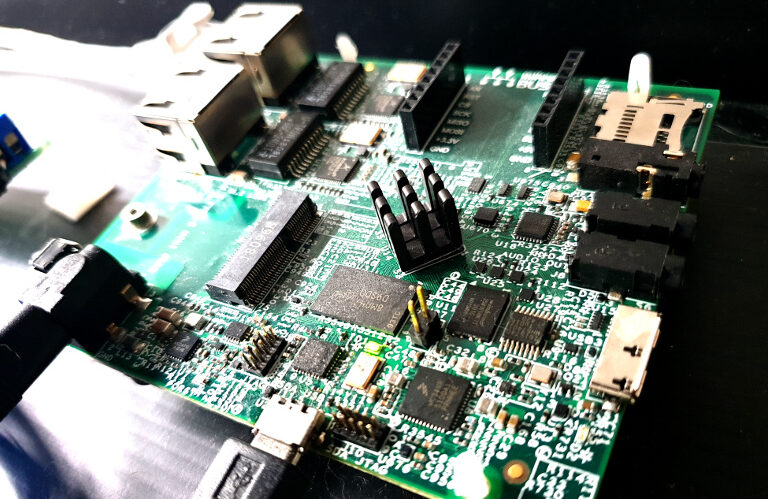
We’ve recently provided software support to Analogue & Micro who are developing hardware derived from NXP’s Layerscape FRWY-LS1012A reference design. What we find interesting about this reference design is that for storage it uses an innovative SPI memory known as SpiStack Flash. Essentially it’s a single chip with a quad-SPI interface, but inside are two (or more) memory dies with an additional SPI command that allows you to switch between them. Those memory die’s don’t need to be homogeneous, thus allowing for parts that, for example have both a NOR die and a NAND die. One of the benefits of these Multi Chip Packages (MCP) is that it allows the product designer to blend the trade-offs between NAND and NOR memories and to do so without sacrificing valuable space on the PCB. In this post we’ll explain the challenges we faced when adding U-Boot and Linux support for the NAND die of a SpiStack part in NXP’s LSDK.
The FRWY reference board uses Winbond’s W25M161AW SpiStack chip – this provides us with a 16 Mbit NOR die (W25Q16JV) and a 1 Gbit NAND die (W25N01GV) – these are the sames dies found in the non SpiStack packages with the same names. Thus, so long as the correct die is active/selected, then any existing software which supports these chips ought to ‘just work’. The default active die on our SpiStack is the NOR, and as a result the LS1012A will happily boot from it just as if it were a non-SpiStack part (W25Q16JV). Unfortunately, out of the box NXP’s LSDK (20.04 and 20.12) doesn’t offer support for the NAND part – it turns out that, due to factors outside the SpiStack chip, it’s not as simple as issuing an SPI command to switch the active die to the NAND.
Let’s start by looking at the ‘Software Die Select (C2h)’ command – this is the special SPI command that is used to select the active die. In reality this just determines which die has control of the SPI bus. (It’s possible to start an operation on one die, and then switch to another die and start an operation there – thus allowing for concurrent use.) In terms of software support, this command has been supported in both Linux and UBoot since support was first added for SPI NANDs back in 2018. However, it appears that the support was intended for homogeneous devices, i.e., where the capacity of a NAND chip was increased by using multiple dies of the same memory organisation. In this context, the existing logic has arithmetic that converts an absolute offset in the logical SpiStack device to an offset within a specific NAND die (nanddev_pos_next_lun) – it also has logic for then selecting that die using the ‘Software Die Select’ command (spinand_select_target). It’s trivial to make use of this existing functionality to provide a means of selecting between the NAND and NOR dies of our SpiStack flash – this is the easy part.
The challenge arises from the QuadSPI controller that the SpiStack chip is connected to on the LS1012A. This isn’t a simple SPI controller designed for general use – it’s a dedicated SPI controller designed for talking to memory chips with good performance and flexibility. Let’s illustrate this with an example – in order to read data from an SPI chip you need to transact SPI commands – in the case of the Winbond NOR die this takes the form of an instruction byte (03h for a read), followed by a 24-bit address, followed by dummy bytes where we clock out as much data as we want to read. One way to achieve this would be to use the memory-mapped registers of a SPI controller to point it to our command bytes and to tell it to start. We’d then need to wait until it’s complete and read back the returned buffer. All of this requiring some software of course. The QuadSPI controller however, offers memory-mapped read access to the SPI memory – in other words a large portion of the processors address space is mapped to the QuadSPI controller so when you read from it the QuadSPI controller will transparently translate that into SPI commands and transact them on your behalf – giving the impression that the SPI memory is mapped into the processor address space. (In exactly the same way that reading a PCI memory address transparently results in the PCI controller sending packets on the PCI bus). This offers many benefits, for example allowing you to boot directly from an SPI memory and allowing you access it via DMA. The controller has a buffer which also improves performance by avoiding unnecessary reading of the SPI memory.
Of course, if the QuadSPI controller is going to transparently send SPI transactions on our behalf then it needs to know which commands to send – and this may vary across vendors and flash technologies. To overcome this the QuadSPI controller makes use of a hardware Look-up-Table (LUT) – this is essentially a table of programmable command sequences. When the processor reads from the memory-mapped area then the controller will issue a command from a pre-specified entry in the look up table. (Out of reset the QuadSPI controller has default values that allow it to read from most common devices). All interactions with the SPI memory occurs through the LUT table. For example if software wanted to send an erase command, it would still have to tell the QuadSPI controller to execute a command from the LUT – rather than specifying the bytes directly.
This brings us to the first challenge – the command sets used by NOR and NAND chips are different yet the size of the LUT is too small to fit in both sets. Regardless, the QuadSPI driver must be modified to update the LUT table and to ensure the correct command is executed as required by the NAND/NOR driver stacks. As an example a typical software stack for an SPI controller may have an ‘xfer‘ function that takes a pointer to a buffer of bytes to send and receive – the SPI driver doesn’t care what these bytes are, it just sends them. With the QuadSPI controller the driver needs to have an understanding of what the commands are such that it can determine which entry of the LUT table to invoke. For example, if you wanted to issue the ‘Read JEDEC ID (9Fh)’ SPI command to find out the ID of the flash chip, the xfer function of the QuadSPI driver must peek into the first byte that is requested to be sent, identify that the first byte is 0x9F and thus the Read JEDEC ID command, identify which entry it uses in the LUT for sending the Read JEDEC ID command – and finally tell the QuadSPI controller to issue that command. In this way supporting differing chips adds a burden of support.
The way we overcame this was to use a newer version of the driver that uses a single entry in the LUT which is programmed before each command – thus allowing us to use the QuadSPI controller like a traditional SPI controller with a minimal understanding about the commands its actually sending on the wire.
The next challenge was handling existing code that relies on memory-mapped access to the NOR memory – for example we found that U-Boot would directly read the memory associated with the NOR when accessing the U-Boot environment (rather than through the spi-mem framework). We also found that the PFE network firmware did the same thing. This is problematic as we don’t want the QuadSPI controller sending commands for the NOR die when we have the NAND die active. Ideally access to the SpiStack chip would be arbitrated in software to ensure we always have the correct die selected. We overcame this challenge by disabling the memory-mapped access to the SPI memory and updating the code to use the spi-mem framework (which explicitly tells the QuadSPI controller to issue a command from the LUT rather than directly read from a memory address range).
Once we overcame these challenges we then needed to update the device tree and kernel/U-Boot configuration to specify that we have a NAND chip and to include the relevant software frameworks. Thus allowing those frameworks to detect and probe the NAND and NOR dies and present them to the user. In the case of U-Boot the ‘mtd‘ commands were needed instead of the older ‘nand‘ commands as the ‘nand’ commands relate solely to raw NAND devices (non-SPI).
Eventually we were able to make use of NAND and NOR in both U-Boot and Linux, horray:
=> mtd list
 List of MTD devices:
 spi-nand0
 device: spi-nand@1
 parent: quadspi@1550000
 driver: spi_nand
 type: NAND flash
 block size: 0x20000 bytes
 min I/O: 0x800 bytes
 OOB size: 64 bytes
 OOB available: 24 bytes
 0x000000000000-0x000008000000 : "spi-nand0"
 nor0
 type: NOR flash
 block size: 0x1000 bytes
 min I/O: 0x1 bytes
 0x000000000000-0x000000200000 : "nor0"
 =>
When we first approached this work we anticipated simply adding code to send an SPI command to switch between NAND and NOR – however we ended up learning about the QuadSPI controller and the NOR, NAND and SPI frameworks in both U-Boot and Linux. We’re happy to have found a solution for Analogue & Micro and along the way gained support for NAND on the FRWY board.